Part 6 — Inference Fundamentals
Inside an NVIDIA GPU: a visual tour
Build a picture of what is physically inside the chip that runs your model — cores, tensor cores, and the memory hierarchy — so that the spec-sheet numbers, the two inference phases, and every kernel trick you meet later stop being magic and start being consequences of the hardware.
You have been told inference is "compute-bound in prefill, memory-bound in decode," that tensor cores do the matrix multiplies, and that FlashAttention wins by "staying in fast memory." Every one of those statements is a fact about a picture — the physical layout of an NVIDIA GPU. This chapter draws that picture. Once you can see the chip, the spec sheet in the next chapter reads itself, and the kernel tricks later stop being folklore.
What you will understand by the end
- Why a GPU looks nothing like a CPU, and what that trade buys.
- The hierarchy inside the die: GPU → streaming multiprocessors (SMs) → cores and tensor cores.
- The memory hierarchy — registers, shared memory/L1, L2, HBM — and the enormous speed gaps between its levels.
- How every one of those structures maps onto prefill, decode, and batching.
CPU versus GPU: two different bets
A CPU and a GPU are built to win opposite races. A CPU has a few very fast cores with huge caches and elaborate control logic, tuned to finish one thread as quickly as possible — it optimises latency. A GPU spends the same silicon on thousands of small cores, tuned to keep many threads in flight and hide waiting with more work — it optimises throughput.
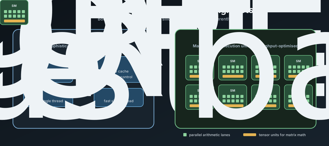
A GPU does not make any single operation fast; it makes an enormous number of identical operations happen at once. Matrix multiplication — the core of a Transformer — is exactly "the same multiply, a billion times," which is why it maps onto this hardware so well and why an LLM on a CPU is so slow.
The die: SMs, cores and tensor cores
Zoom into the GPU die and you find it is tiled with dozens of identical blocks called streaming multiprocessors (SMs) — an H100 has 132 of them. The SM is the real unit of a GPU: the whole chip is "an SM, copied ~130 times, sharing an L2 cache and memory."

Two kinds of math unit live in each SM:
- CUDA cores — plain scalar ALUs that do one floating-point (or integer) operation each. They handle the general-purpose arithmetic: activations, normalisation, the element-wise glue between big operations.
- Tensor cores — specialised units that multiply small matrices in a single instruction rather than one number at a time. This is where the FLOPS on the spec sheet come from, and it is why the numbers explode as precision drops (a tensor core chews through far more FP8 or FP4 elements per cycle than FP16).
The tensor cores are the inference engine. A Transformer is a stack of large matrix multiplies (attention scores, projections, the MLP), and those land on tensor cores. When people say a GPU is "fast at AI," they mean it has tensor cores — and when prefill is "compute-bound," it means prefill is saturating the tensor cores.
That "same SM, stamped out dozens of times" design also explains a pricing puzzle you will meet in the next chapter. Because the die is one block repeated, a manufacturing defect usually kills a single SM rather than the whole chip — so the vendor disables the broken block and sells that die as a lower tier with fewer working SMs. The identical physical chip can ship as several products (this is called binning) that differ mainly in how many SMs survived and at what clock. It is a big reason that, within one generation, a bigger model number is often just the same silicon with more cores switched on — the point the spec-sheet chapter makes about the "letter versus number."
The memory hierarchy: the gaps are everything
The math units are only ever as useful as the data you can feed them. Memory on a GPU is a pyramid: tiny and blindingly fast at the top, huge and comparatively slow at the bottom — and the speed gaps between levels are the single most important thing to internalise, because almost every optimisation is about staying near the top.
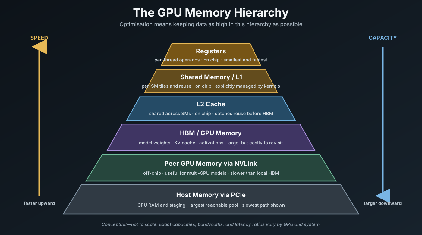
The numbers are approximate and generation-dependent, but the shape is the lesson: HBM — the "80 GB" or "141 GB" on the spec sheet — is the biggest pool the math units can reach directly, yet it is 10–100× slower than the on-chip scratchpads. Getting a byte from HBM costs hundreds of cycles; the tensor cores could have done hundreds of multiplies in that time.
"VRAM" hides two very different numbers that people constantly merge: capacity (how many GB of weights + KV cache fit) and bandwidth (how fast HBM streams into the SMs). Capacity caps your batch size and context length; bandwidth caps your decode speed. They live on the same line of the spec sheet and mean completely different things — the next chapter, reading a GPU spec sheet, turns this split into a buying decision.
Warps and SIMT: how work fills the SMs
An SM does not run your program one thread at a time. Work is issued as threads, bundled into warps of 32 that share a single instruction stream, grouped into blocks (a whole block runs on one SM, so its threads can share that SM's L1/shared memory), and finally a grid spread across the whole GPU. A hardware scheduler sprays blocks onto whichever SMs are free. Modern NVIDIA GPUs run this as SIMT — single instruction, multiple threads — where the 32 threads move together but each keeps its own state, so they can take different branches and re-converge rather than march in rigid lockstep.
Two facts from this execution model drive inference performance directly:
- Occupancy is how an SM hides the HBM latency. The SM stays busy by keeping many warps ready and switching to another the instant one stalls on memory. If there is not enough independent work — batch-size-1 decode is the textbook case — most warp slots sit empty and the SM simply waits on HBM with nothing to overlap. That is the hardware reason batching turns a stalled SM into a saturated one.
- Threads in a block cooperate through shared memory. Because a block's threads share the on-chip L1/shared memory, they can pass results to one another without a trip to HBM. That is exactly the move FlashAttention makes: keep the attention tile in shared memory and let the warps work on it together, instead of streaming the large score matrix down to HBM and back.
A GPU only runs fast when it has enough independent work to fill the warps and that work reuses on-chip memory. Occupancy (fed by batching) and shared-memory cooperation (exploited by good kernels) are the two levers — which is why the same card can look idle on one workload and fully saturated on another.
Why this picture explains everything downstream
Every inference fact you have met or will meet is a shadow of this diagram:
- Prefill is compute-bound. Reading a long prompt is one big matrix multiply that keeps the tensor cores busy — the SMs are the bottleneck, HBM has slack. See Prefill and decode.
- Decode is memory-bound. Emitting one token re-reads all the model's weights from
HBM to do a comparatively tiny multiply. The tensor cores sit idle waiting on HBM
bandwidth — that is why
tokens/sec ≈ bandwidth ÷ model size. - Batching exists to fill the SMs. At batch size 1, decode barely lights up the thousands of cores. Batching many requests reuses the same weight read across many tokens, converting a bandwidth-bound trickle into compute the SMs can chew — the subject of batching and concurrency.
- Kernel tricks fight the memory pyramid. FlashAttention is fast because it keeps attention tiles in shared memory instead of round-tripping through HBM; kernel fusion exists to avoid writing intermediate results down to HBM and reading them back. This is what CUDA and kernels is really about.
- Quantization shrinks what must cross the gap. Fewer bits per weight means fewer bytes streamed from HBM per token (faster decode) and more tensor-core throughput — see Quantization.
This project's serving experiments run on a single L4 — a small GPU with tensor cores but no NVLink. Under load its KV cache (which lives in HBM) sat near 1.4% full while the SMs were busy: the workload was compute-bound at the tensor cores, not starved on HBM capacity. The picture predicted the measurement. Read the serving-knobs experiment →
Mental model
A GPU is ~130 identical SMs — each a bundle of CUDA cores plus tensor cores over a tiny fast scratchpad — all fed from one big, comparatively slow pool of HBM. Inference performance is the story of keeping the tensor cores busy and minimising trips down to HBM. Everything else is detail.
Common mistakes
- Thinking of a GPU as "a fast CPU." It is the opposite bet: slow per-thread, absurdly parallel. Code (and mental models) written for one core do not transfer.
- Ignoring the memory pyramid. Treating HBM as "the memory" hides the 10–100× cliff between it and on-chip scratchpad — the cliff every kernel optimisation is fighting.
- Conflating capacity and bandwidth. "It has 80 GB" tells you what fits, not how fast it decodes. They are different axes with different bottlenecks.
- Assuming more cores means more speed for your job. If decode is waiting on HBM, extra idle SMs do nothing — you needed bandwidth (or batching), not cores.
Practical guidance
- When you read a GPU spec, sort every number into the pyramid: FLOPS = tensor-core throughput (prefill), TB/s = HBM bandwidth (decode), GB = HBM capacity (batch/context).
- To reason about a slow workload, ask which level of the pyramid it is stuck on before reaching for a bigger card — the fix is often a config or kernel change, not silicon.
- Remember the SM is the unit: "utilisation" means "fraction of SMs (and their tensor cores) doing work," which is why low batch sizes look busy but idle.
- Carry this diagram into the next chapters — it is the substrate under the spec sheet, the KV cache, batching, and parallelism alike.
Summary
- A GPU trades single-thread speed for massive parallelism: ~130 SMs, each packed with CUDA cores and tensor cores (the matmul units that are the FLOPS).
- Memory is a pyramid — registers → shared/L1 → L2 → HBM → NVLink → host — with order-of-magnitude speed cliffs at each step; HBM is the big-but-slow pool the math units live on.
- Prefill saturates tensor cores (compute-bound); decode waits on HBM bandwidth (memory-bound); batching and kernel tricks exist to fill the SMs and dodge the HBM cliff.
- Read the spec sheet, the KV cache, and every optimisation as consequences of this one picture.
Knowledge check
Decode is slow but GPU "utilisation" looks low and there is plenty of free VRAM. Using the pyramid, what is the bottleneck and what is the fix?
Decode re-reads all the weights from HBM for each token, so it is bound by HBM bandwidth, not capacity or compute — which is exactly why the SMs (utilisation) look idle and VRAM looks free. The fix is not a bigger card or more cores; it is batching (reuse each weight read across many concurrent tokens) so the bandwidth you are already paying for produces more work.
Why does FlashAttention count as a "memory hierarchy" optimisation rather than a "do less math" one?
It does roughly the same arithmetic; its win is where the data lives. Naive attention writes the large intermediate score matrix down to HBM and reads it back; FlashAttention keeps tiles in on-chip shared memory/registers and never materialises the full matrix in HBM, avoiding the slow trips down the pyramid. It is a data-movement win, not a FLOPS win.
Related chapters
- GPU architecture and inference hardware — turning this picture into a spec-sheet buying decision
- Prefill and decode — the two phases this hardware splits inference into
- CUDA and kernels — the software that fights the memory pyramid
- Model parallelism and distributed inference — when one die is not enough, and NVLink stitches many together